-
13.
The channel resistance of an N – channel JFET shown in the figure below is 600Ω when the full channel thickness (tch) of 10μm is available for conduction. The built – in voltage of the gate P+N junction (Vbi) is -1V. When the gate to source voltage (VGS) is 0 V, the channel is depleted by 1 μm on each side due to the built – in voltage and hence the thickness available for conduction is only 8μm.
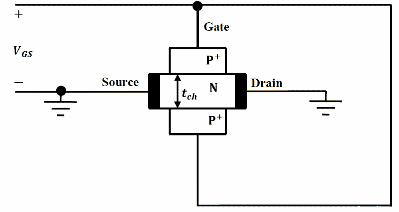
[1] The channel resistance when VGS = 0V is : [2 marks]
(A) 480Ω
(B) 600Ω
(C) 750Ω
(D) 1000Ω[2] The channel resistance when VGS = -3V is : [2 marks]
(A) 360Ω
(B) 917Ω
(C) 1000Ω
(D) 3000Ωlast reply by CpjJwWHV • 12 years ago • asked in Electronics and Communication Engineering, 2011
View Comments [1 Reply]
-
14.
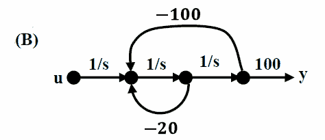
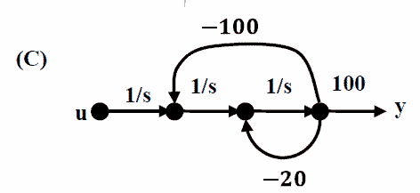
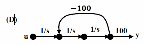
The input – output transfer function of a plant H(S) = 100/[s(s+10)2]. The plant is placed in a unity negative feedback configuration as shown in the figure below.
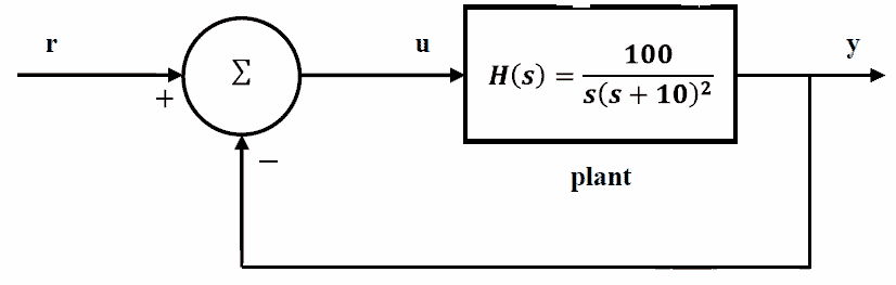
[1] The signal flow graph that DOES NOT model the plant transfer function H(S) is : [2 marks] 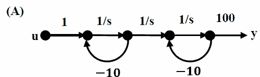
[2] The gain margin of the system under closed loop unity negative feedback is
[2 marks]
(A) 0 dB
(B) 20 dB
(C) 26 dB
(D) 46 dBasked in Electronics and Communication Engineering, 2011
View Comments [0 Reply]
-
15.
-
16.
-
17.
-
18.