-
403.
Statement for Linked Answer Questions::
The following two questions refer to wide sense stationary stochastic processes.[1] It is desired to generate a stochastic process (as voltage process) with power spectral density.
s(ω) = 16/(16+ω2)
By driving a Linear-Time-Invariant system by zero mean white noise (as voltage process) with power spectral density being constant equal to 1. The system which can perform the desired task could be: [2 marks]
(A) first order lowpass R-L filter
(B) first order highpass R-c filter
(C) tuned L-C filter
(D) series R-L-C filter
[2] The parameters of the system obtained in above question would be
[2 marks]
(A) first order R-L lowpass filter would have R = 4Ω, L = 4H
(B) first order R-C highpass filter would have R = 4Ω, C = 0.25F
(C) tuned L-C filter would have L = 4H, C = 4F
(D) series R-L-C lowpass filter would have R = 1Ω,, L = 4H, C = 4Fasked in Electronics and Communication Engineering, 2006
View Comments [0 Reply]
-
404.
Statement for Linked Answer Questions:
A regulated power supply, shown in figure below, has an unregulated input (UR) of 15 Volts and generates a regulated output Vout. Use the component values shown in the figure.
In the figure above, the ground has been shown by the symbol ∇.[1] The power dissipation across the transistor Q1 shown in the figure is:
[2 marks]
(A) 4.8 Watts
(B) 5.0 Watts
(C) 5.4 Watts
(D) 6.0 Watts[2] If the unregulated voltage increases by 20%, the power dissipation across the transistor Q1 [2 marks]
(A) increases by 20%
(B) increases by 50%
(C) remains unchanged
(D) decreases by 20%asked in Electronics and Communication Engineering, 2006
View Comments [0 Reply]
-
405.
Let g (t) = p (t) * p (t) ,where * denotes convolution and p (t) = u (t)−u(t−1) with u (t) being the unit step function.
[1] The impulse response of filter matched to the signal s (t) = g(t)−δ(t − 2)*g(t) is given as: [2 marks]
(A) s (1 − t )
(B) −s (1 − t )
(C) −s (t )
(D) s (t )[2] An Amplitude Modulated signal is given as
XAM(t) = 100 (p(t)+0.5g(t)) cosωct
in the interval 0 ≤ t ≤ 1. One set of possible values of the modulating signal and modulation index would be [2 marks]
(A) t,0.5
(B) t,1.0
(C) t,2.0
(D) t2 ,0.5
asked in Electronics and Communication Engineering, 2006
View Comments [0 Reply]
-
406.
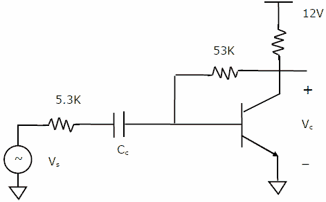
In the transistor amplifier circuit shown in the figure below, the transistor has the following parameters:
βDC = 60, VBE = 0.7V, hie→∞, hfe→∞.
The capacitance Cc can be assumed to be infinite.
In the figure above, the ground has been shown by the symbol ∇.[1] Under the DC conditions, the collector-to-emitter voltage drop is: [2 marks]
(A) 4.8 Volts
(B) 5.3 Volts
(C) 6.0 Volts
(D) 6.6 Volts[2] If βDC is increased by 10%, the collector-to-emitter voltage drop
[2 marks]
(A) increases by less than or equal to 10%
(B) decreases by less than or equal to 10%
(C) increases by more than 10%
(D) decreases by more than 10%
[3] The small-signal gain of the amplifier vc/vs is :[2 marks]
(A) -10
(B) -5.3
(C) 5.3
(D) 10
asked in Electronics and Communication Engineering, 2006
View Comments [0 Reply]
-
407.
-
408.
