-
475.
-
476.
-
477.
Statement for Linked Answer Questions ::
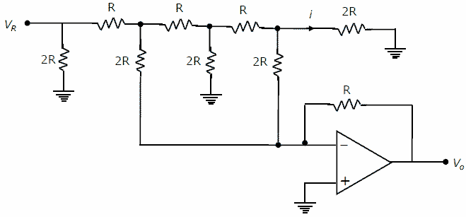
In the Digital-to-Analog converter circuit shown in the figure below, VR = 10V and R = 10KΩ.
[1] The current i is: [2 marks]
(A) 31.25 µA
(B) 62.5 µA
(C) 125 µA
(D) 250 µA[2] The voltage Vo is: [2 marks]
(A) -0.781 V
(B) -1.562 V
(C) -3.125 V
(D) -6.250 Vasked in Electronics and Communication Engineering, 2007
View Comments [0 Reply]
-
478.
Statement for Linked Answer Questions ::
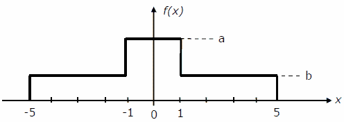
An input to a 6-level quantizer has the probability density function f (x) as shown in the figure. Decision boundaries of the quantizer are chosen so as t maximize the entropy of the quantizer output. It is given that 3 consecutive decision boundaries are ‘-1’, ‘0’ and ‘1’.
[1] The values of a and b are: [2 marks]
(A) a= 1/6 and b=1/12
(B) a= 1/5 and b=3/40
(C) a= 1/4 and b=1/16
(D) a= 1/3 and b=1/24
[2] Assuming that the reconstruction levels of the quantizer are the mid-points of the decision boundaries, the ratio of signal power to quantization noise power is: [2 marks]
(A) 152/9
(B) 64/3
(C) 76/3
(D) 28
asked in Electronics and Communication Engineering, 2007
View Comments [0 Reply]
-
479.
Statement for Linked Answer Questions ::
Consider a linear system whose state space representation is x(t) = Ax(t). If the initial state vector of the system is , then the system response is
 .If the initial state vector of the system changes to
  , then the system response becomes
  .
.
[1] The eigenvalue and eigenvector pairs (λi, vi) for the system are
[2 marks]
[2] The system matrix A is: [2 marks] 
asked in Electronics and Communication Engineering, 2007
View Comments [0 Reply]
-
480.
Statement for Linked Answer Questions:
An 8085 assembly language program is given below.
Line 1: MVI A, B5H
2: MVI B, 0EH
3: XRI 69H
4: ADD B
5: ANI 9BH
6: CPI 9FH
7: STA 3010H
8: HLT[1] The contents of the accumulator just after execution of the ADD instruction in line 4 will be [2 marks]
(A) C3H
(B) EAH
(C) DCH
(D) 69H[2] After execution of line 7 of the program, the status of the CY and Z flags will be [2 marks]
(A) CY = 0, Z = 0
(B) CY = 0, Z = 1
(C) CY = 1, Z = 0
(D) CY = 1, Z = 1asked in Electronics and Communication Engineering, 2007
View Comments [0 Reply]
