-
481.
Statement for Linked Answer Questions ::
Consider the Op-Amp circuit shown in the figure.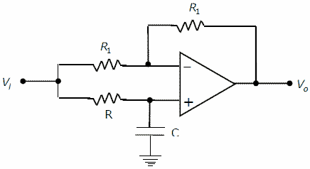
[1] The transfer function Vo(s)/Vi(s) is : [2 marks]
(A) (1-sRC)/(1+sRC)
(B) (1+sRC)/(1-sRC)
(C) 1/(1-sRC)
(D) 1/(1+sRC)
[2] If Vi = V1sin(ωt) and Vo = V2sin(ωt+φ)then the minimum and maximum values of φ (in radians) are respectively [2 marks]
(A) -π/2 and π/2
(B) 0 and π/2
(C) -π and 0
(D) -π/2 and 0
asked in Electronics and Communication Engineering, 2007
View Comments [0 Reply]
-
482.
Two 4-ray signal constellations are shown. It is given that φ1 and φ2 constitute an orthonormal basis for the two constellations. Assume that the four symbols in both the constellations are equiprobable. Let No/2 denote the power spectral density of white Gaussian noise.
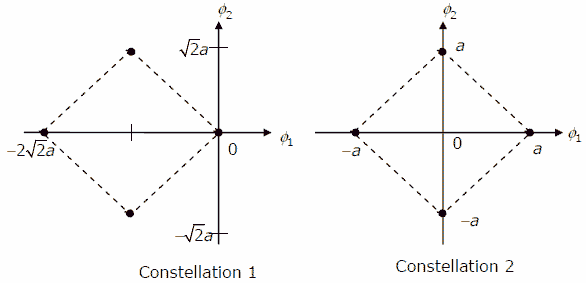
[1] The ratio of the average energy of Constellation 1 to the average energy of Constellation 2 is: [2 marks]
(A) 4a2
(B) 4
(C) 2
(D) 8[2] If these constellations are used for digital communications over an AWGN channel, then which of the following statements is true? [2 marks]
(A) Probability of symbol error for Constellation 1 is lower
(B) Probability of symbol error for Constellation 1 is higher
(C) Probability of symbol error is equal for both the constellations
(D) The value of No will determine which of the two constellations has a lower probability of symbol error.asked in Electronics and Communication Engineering, 2007
View Comments [0 Reply]
-
483.
The figure shows the high-frequency capacitance-voltage (C-V) characteristics of a Metal/SiO2 /silicon (MOS) capacitor having an area of 1x10⁻⁴ cm2. Assume that the permitivities (εoεr) of silicon and SiO2 are 1x10-12 F/cm and 3.5x10⁻¹³ F/cm respectively.

[1] The gate oxide thickness in the MOS capacitor is: [2 marks]
(A) 50 nm
(B) 143 nm
(C) 350 nm
(D) 1 µm[2] The maximum depletion layer width in silicon is [2 marks]
(A) 0.143 µm
(B) 0.857 µm
(C) 1 µm
(D) 1.143 µm[3] Consider the following statements about the C-V characteristics plot:
S1: The MOS capacitor has an n-type substrate.
S2: If positive charges are introduced in the oxide, the C-V plot will shift to the
left.
Then which of the following is true? [2 marks]
(A) Both S1 and S2 are true
(B) S1 is true and S2 is false
(C) S1 is false and S2 is true
(D) Both S1 and S2 are falseasked in Electronics and Communication Engineering, 2007
View Comments [0 Reply]
-
484.
-
485.
-
486.

