-
1.
Statement for Linked Answer Questions ::
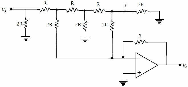
In the Digital-to-Analog converter circuit shown in the figure below, VR = 10V and R = 10KΩ.
[1] The current i is: [2 marks]
(A) 31.25 µA
(B) 62.5 µA
(C) 125 µA
(D) 250 µA[2] The voltage Vo is: [2 marks]
(A) -0.781 V
(B) -1.562 V
(C) -3.125 V
(D) -6.250 Vasked in Electronics and Communication Engineering, 2007
View Comments [0 Reply]
-
2.
Statement for Linked Answer Questions ::
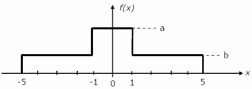
An input to a 6-level quantizer has the probability density function f (x) as shown in the figure. Decision boundaries of the quantizer are chosen so as t maximize the entropy of the quantizer output. It is given that 3 consecutive decision boundaries are ‘-1’, ‘0’ and ‘1’.
[1] The values of a and b are: [2 marks]
(A) a= 1/6 and b=1/12
(B) a= 1/5 and b=3/40
(C) a= 1/4 and b=1/16
(D) a= 1/3 and b=1/24
[2] Assuming that the reconstruction levels of the quantizer are the mid-points of the decision boundaries, the ratio of signal power to quantization noise power is: [2 marks]
(A) 152/9
(B) 64/3
(C) 76/3
(D) 28
asked in Electronics and Communication Engineering, 2007
View Comments [0 Reply]
-
3.
Statement for Linked Answer Questions ::
Consider a linear system whose state space representation is x(t) = Ax(t). If the initial state vector of the system is , then the system response is
 .If the initial state vector of the system changes to
  , then the system response becomes
  .
.
[1] The eigenvalue and eigenvector pairs (λi, vi) for the system are
[2 marks]
[2] The system matrix A is: [2 marks] 
asked in Electronics and Communication Engineering, 2007
View Comments [0 Reply]
-
4.
Statement for Linked Answer Questions:
An 8085 assembly language program is given below.
Line 1: MVI A, B5H
2: MVI B, 0EH
3: XRI 69H
4: ADD B
5: ANI 9BH
6: CPI 9FH
7: STA 3010H
8: HLT[1] The contents of the accumulator just after execution of the ADD instruction in line 4 will be [2 marks]
(A) C3H
(B) EAH
(C) DCH
(D) 69H[2] After execution of line 7 of the program, the status of the CY and Z flags will be [2 marks]
(A) CY = 0, Z = 0
(B) CY = 0, Z = 1
(C) CY = 1, Z = 0
(D) CY = 1, Z = 1asked in Electronics and Communication Engineering, 2007
View Comments [0 Reply]
-
5.
Statement for Linked Answer Questions ::
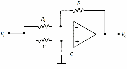
Consider the Op-Amp circuit shown in the figure.
[1] The transfer function Vo(s)/Vi(s) is : [2 marks]
(A) (1-sRC)/(1+sRC)
(B) (1+sRC)/(1-sRC)
(C) 1/(1-sRC)
(D) 1/(1+sRC)
[2] If Vi = V1sin(ωt) and Vo = V2sin(ωt+φ)then the minimum and maximum values of φ (in radians) are respectively [2 marks]
(A) -π/2 and π/2
(B) 0 and π/2
(C) -π and 0
(D) -π/2 and 0
asked in Electronics and Communication Engineering, 2007
View Comments [0 Reply]
-
6.
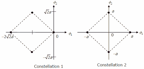
Two 4-ray signal constellations are shown. It is given that φ1 and φ2 constitute an orthonormal basis for the two constellations. Assume that the four symbols in both the constellations are equiprobable. Let No/2 denote the power spectral density of white Gaussian noise.

[1] The ratio of the average energy of Constellation 1 to the average energy of Constellation 2 is: [2 marks]
(A) 4a2
(B) 4
(C) 2
(D) 8[2] If these constellations are used for digital communications over an AWGN channel, then which of the following statements is true? [2 marks]
(A) Probability of symbol error for Constellation 1 is lower
(B) Probability of symbol error for Constellation 1 is higher
(C) Probability of symbol error is equal for both the constellations
(D) The value of No will determine which of the two constellations has a lower probability of symbol error.asked in Electronics and Communication Engineering, 2007
View Comments [0 Reply]
